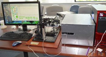

Integrated spectrometer & 3D imager
Applied Research & Photonics
Main features - Fine scale inspection: a resolution of 25 nm - Layer by layer non-destructive inspection - Scanning area: up to 200 mm by 200 mm (can be tailored to other sizes) - Scanning speed: currently 10 mm/s (max) (can be increased per need) - Simultaneous reflection and transmission measurements - Reconstructive 3D imaging (no camera needed) A paper for wafer inspection is here: Effective testing for wafer reject minimization by terahertz analysis and sub-surface imaging
*Manufacturer's specifications subject to change without notice.
Leading terahertz instrument maker. Products:
- Integrated terahertz scanning spectrometer/3D imager
- Terahertz time-domain spectrometer (TeraSpectra©)
- Sub-surface nanoscanner and 3D imager
- Scanning reflectometer for skin scanner and thickness profiling
- Ballistic helmet analyzer
- Terahertz reflective interferometer for paint and coating layer analyzing.
View Products
Company Website
Contact
